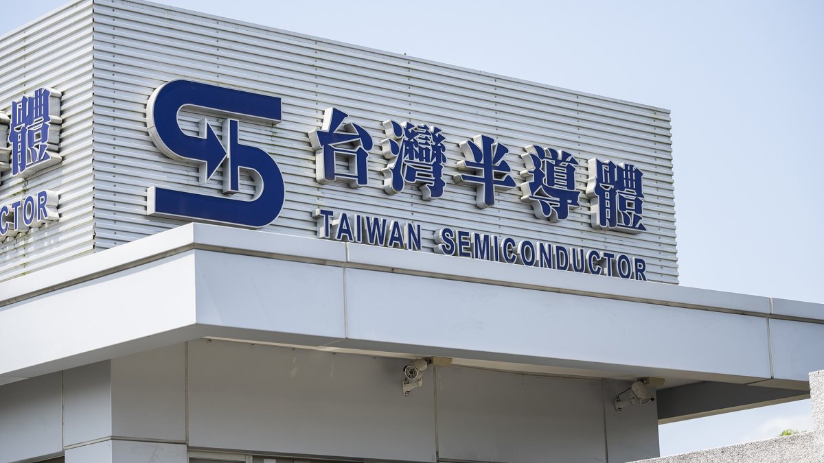
Japan has formally approved TSMC's plan to build 3-nanometer chips at its second fab in Kumamoto Prefecture, clearing the way for the country's first advanced-node logic production. Japan's Ministry of Economy, Trade and Industry published the approval for the plant run by JASM, TSMC's majority-owned Japanese subsidiary, with Taiwanese trade outlet DigiTimes reporting the decision and Japanese broadcaster TBS noting the ministry signed off on Friday.
The revised plan replaces what was originally earmarked for the site: the second fab had been designed around 40nm, 12nm and 6nm processes with a combined design capacity of 63,000 wafers a month. It will now focus on 3nm output of 6,000 wafers per month, with construction expected to finish and production to begin in December 2028. DigiTimes reports first shipments are pencilled in for the fourth quarter of 2028.
Fewer wafers does not mean a smaller project. A 3nm wafer carries far more value than a mature-node one, and the Japanese government has matched the upgrade with money: the approved subsidy ceiling for the second fab is 645.15 billion yen, roughly 4.1 billion dollars. With incentives for the first fab included, Japanese support for the two-plant campus is expected to exceed one trillion yen.
The shift had been signaled for months. In February 2026, TSMC Chairman C.C. Wei discussed the possibility of converting the second Kumamoto plant to 3nm capacity during a meeting with Japan's prime minister, and the project's total investment was raised from about 12.2 billion dollars to 17 billion dollars, according to industry reports at the time. The stated driver is AI: demand for leading-edge logic has crowded out the original mature-node roadmap.
The first Kumamoto fab, which opened in February 2024 and entered mass production at the end of that year, is also being reorganized. It will abandon its planned 12/16nm lines and concentrate on 45,000 wafers a month of 22/28nm output plus 5,000 wafers of 40nm, with commitments to supply Japanese customers for at least ten years. JASM is owned roughly 86.5 percent by TSMC, 6 percent by Sony, 5.5 percent by Denso and 2 percent by Toyota.
The approval puts Japan on the advanced-node map for the first time. Japanese logic production had previously topped out around the 40nm to 28nm range, and the government has positioned Kumamoto's 3nm as complementary to Rapidus, the domestic venture racing toward 2nm rather than competing at the same node. It is worth keeping in mind that 3nm is not TSMC's leading edge either: the company put 2nm into high-volume manufacturing in the fourth quarter of 2025, and 3nm accounted for about 24 percent of its 2025 wafer revenue.
For TSMC, the move adds a second geography for an established process at a moment when customers are asking for supply outside Taiwan. For Japan, it means AI accelerator-class silicon can eventually be made domestically rather than imported as finished chips. The 6,000-wafer figure is planned capacity, not current output, and the real test will be whether the 2028 timeline holds and whether Japanese demand for 3nm materializes at the scale the subsidy assumes.
Comments (0)
Log in to join the discussion
Log InNo comments yet